- 您现在的位置:买卖IC网 > Sheet目录3879 > PIC18F65J11-I/PT (Microchip Technology)IC PIC MCU FLASH 16KX16 64TQFP
PIC18F85J11 FAMILY
DS39774D-page 130
2010 Microchip Technology Inc.
Table 11-2 summarizes the output capabilities of the
ports. Refer to the “Absolute Maximum Ratings” in
details.
TABLE 11-2:
OUTPUT DRIVE LEVELS FOR
VARIOUS PORTS
11.1.3
PULL-UP CONFIGURATION
Four of the I/O ports (PORTB, PORTD, PORTE and
PORTJ) implement configurable weak pull-ups on all
pins. These are internal pull-ups that allow floating
digital input signals to be pulled to a consistent level
without the use of external resistors.
The pull-ups are enabled with a single bit for each of the
ports: RBPU (INTCON2<7>) for PORTB, and RDPU,
REPU and RJPU (PORTG<7:5>) for the other ports.
11.1.4
OPEN-DRAIN OUTPUTS
The output pins for several peripherals are also
equipped with a configurable open-drain output option.
This allows the peripherals to communicate with
external digital logic, operating at a higher voltage
level, without the use of level translators.
The open-drain option is implemented on port pins
specifically associated with the data and clock outputs
of the USARTs, the MSSP module (in SPI mode) and
the CCP modules. The option is selectively enabled by
setting the open-drain control bit for the corresponding
module in TRISG and LATG. Their configuration is
discussed in more detail in the sections for PORTC,
PORTE and PORTG.
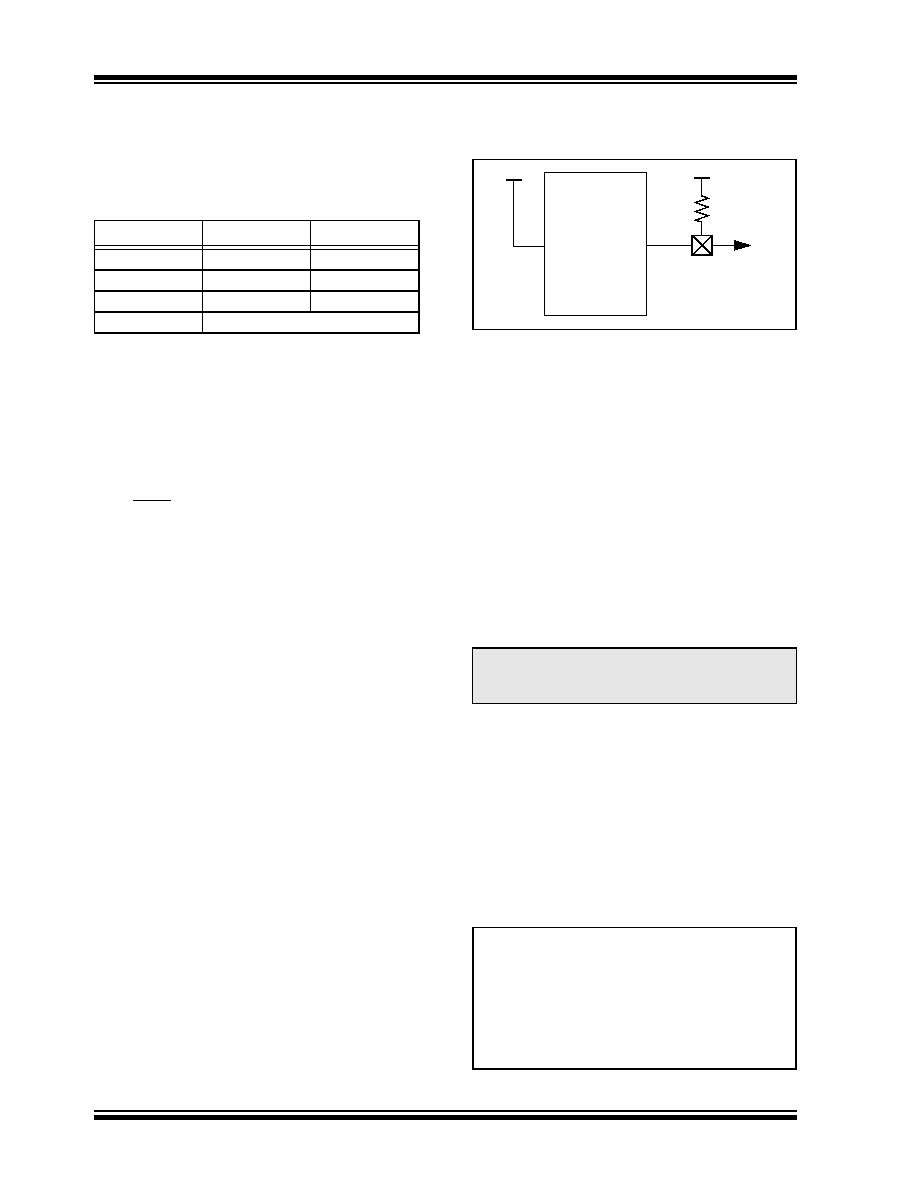
When the open-drain option is required, the output pin
must also be tied through an external pull-up resistor
provided by the user to a higher voltage level, up to 5V
(Figure 11-2). When a digital logic high signal is output,
it is pulled up to the higher voltage level.
FIGURE 11-2:
USING THE OPEN-DRAIN
OUTPUT (USARTs
SHOWN AS EXAMPLES
11.2
PORTA, TRISA and LATA Registers
PORTA is an 8-bit wide, bidirectional port. The corre-
sponding Data Direction and Output Latch registers are
TRISA and LATA.
RA4/T0CKI is a Schmitt Trigger input. All other PORTA
pins have TTL input levels and full CMOS output drivers.
The RA4 pin is multiplexed with the Timer0 clock input.
RA5 and RA<3:0> are multiplexed with analog inputs
for the A/D Converter.
The operation of the analog inputs as A/D Converter
inputs is selected by clearing or setting the PCFG<3:0>
control bits in the ADCON1 register. The corresponding
TRISA bits control the direction of these pins, even
when they are being used as analog inputs. The user
must ensure the bits in the TRISA register are
maintained set when using them as analog inputs.
RA6/OSC2/CLKO and RA7/OSC1/CLKI normally
serve as the external circuit connections for the exter-
nal (primary) oscillator circuit (HS Oscillator modes), or
the external clock input and output (EC Oscillator
modes). In these cases, RA6 and RA7 are not available
as digital I/O and their corresponding TRIS and LAT
bits are read as ‘0’. When the device is configured to
use INTOSC or INTRC as the default oscillator mode
(FOSC2 Configuration bit is ‘0’), RA6 and RA7 are
automatically configured as digital I/O; the oscillator
and clock in/clock out functions are disabled.
EXAMPLE 11-1:
INITIALIZING PORTA
Low
Medium
High
PORTA<5:0>
PORTD
PORTA<7:6>
PORTF
PORTE
PORTB
PORTG
PORTJ(1)
PORTC
PORTH(1)
Note 1:
Not available on 64-pin devices.
Note:
RA5 and RA<3:0> are configured as
analog inputs on any Reset and are read
as ‘0’. RA4 is configured as a digital input.
TXX
PIC18F85J11
+5V
3.3V
(at logic ‘1’)
3.3V
VDD
5V
CLRF
PORTA
; Initialize PORTA by
; clearing output latches
CLRF
LATA
; Alternate method to
; clear output data latches
MOVLW
07h
; Configure A/D
MOVWF
ADCON1
; for digital inputs
MOVLW
0BFh
; Value used to initialize
; data direction
MOVWF
TRISA
; Set RA<7, 5:0> as inputs,
; RA<6> as output
发布紧急采购,3分钟左右您将得到回复。
相关PDF资料
PIC18F2439-E/SO
IC PIC MCU FLASH 6KX16 28SOIC
PIC16LF1938-I/SS
IC MCU 8BIT FLASH 28SSOP
PIC16C621A-20/SO
IC MCU OTP 1KX14 COMP 18SOIC
PIC18F23K22-I/SO
IC PIC MCU 8KB FLASH 28SOIC
PIC18LF2331-I/MM
IC MCU FLASH 4KX16 28QFN
PIC16F639-I/P
IC MCU FLASH 2KX14 20DIP
PIC18F25K20-I/SS
IC PIC MCU FLASH 16KX16 28SSOP
PIC16C58B-04/P
IC MCU OTP 2KX12 18DIP
相关代理商/技术参数
PIC18F65J11T-I/PT
功能描述:8位微控制器 -MCU 32KB Flash 2048bytes-RAM 51I/O RoHS:否 制造商:Silicon Labs 核心:8051 处理器系列:C8051F39x 数据总线宽度:8 bit 最大时钟频率:50 MHz 程序存储器大小:16 KB 数据 RAM 大小:1 KB 片上 ADC:Yes 工作电源电压:1.8 V to 3.6 V 工作温度范围:- 40 C to + 105 C 封装 / 箱体:QFN-20 安装风格:SMD/SMT
PIC18F65J15-I/PT
功能描述:8位微控制器 -MCU 32 KB FL 2KB RAM RoHS:否 制造商:Silicon Labs 核心:8051 处理器系列:C8051F39x 数据总线宽度:8 bit 最大时钟频率:50 MHz 程序存储器大小:16 KB 数据 RAM 大小:1 KB 片上 ADC:Yes 工作电源电压:1.8 V to 3.6 V 工作温度范围:- 40 C to + 105 C 封装 / 箱体:QFN-20 安装风格:SMD/SMT
PIC18F65J15T-I/PT
功能描述:8位微控制器 -MCU 32 KB FL 2KB RAM RoHS:否 制造商:Silicon Labs 核心:8051 处理器系列:C8051F39x 数据总线宽度:8 bit 最大时钟频率:50 MHz 程序存储器大小:16 KB 数据 RAM 大小:1 KB 片上 ADC:Yes 工作电源电压:1.8 V to 3.6 V 工作温度范围:- 40 C to + 105 C 封装 / 箱体:QFN-20 安装风格:SMD/SMT
PIC18F65J50-I/PT
功能描述:8位微控制器 -MCU 32KB FLSH 3936Bs RAM USB 2.0 nanoWatt RoHS:否 制造商:Silicon Labs 核心:8051 处理器系列:C8051F39x 数据总线宽度:8 bit 最大时钟频率:50 MHz 程序存储器大小:16 KB 数据 RAM 大小:1 KB 片上 ADC:Yes 工作电源电压:1.8 V to 3.6 V 工作温度范围:- 40 C to + 105 C 封装 / 箱体:QFN-20 安装风格:SMD/SMT
PIC18F65J50T-I/PT
功能描述:8位微控制器 -MCU 32KB FLSH 3936Bs RAM USB 2.0 nanoWatt RoHS:否 制造商:Silicon Labs 核心:8051 处理器系列:C8051F39x 数据总线宽度:8 bit 最大时钟频率:50 MHz 程序存储器大小:16 KB 数据 RAM 大小:1 KB 片上 ADC:Yes 工作电源电压:1.8 V to 3.6 V 工作温度范围:- 40 C to + 105 C 封装 / 箱体:QFN-20 安装风格:SMD/SMT
PIC18F65J90-I/PT
功能描述:8位微控制器 -MCU 32KB FL 2048b RAM 51I/O 8b Fam RoHS:否 制造商:Silicon Labs 核心:8051 处理器系列:C8051F39x 数据总线宽度:8 bit 最大时钟频率:50 MHz 程序存储器大小:16 KB 数据 RAM 大小:1 KB 片上 ADC:Yes 工作电源电压:1.8 V to 3.6 V 工作温度范围:- 40 C to + 105 C 封装 / 箱体:QFN-20 安装风格:SMD/SMT
PIC18F65J90-I/PT
制造商:Microchip Technology Inc 功能描述:IC MCU 8BIT 32K FLASH SMD TQFP64
PIC18F65J90T-I/PT
功能描述:8位微控制器 -MCU 32KB Flash 2048bytes-RAM 51I/O RoHS:否 制造商:Silicon Labs 核心:8051 处理器系列:C8051F39x 数据总线宽度:8 bit 最大时钟频率:50 MHz 程序存储器大小:16 KB 数据 RAM 大小:1 KB 片上 ADC:Yes 工作电源电压:1.8 V to 3.6 V 工作温度范围:- 40 C to + 105 C 封装 / 箱体:QFN-20 安装风格:SMD/SMT